Etching in Semiconductor Manufacturing: A Deep Dive
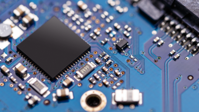
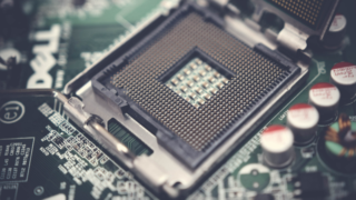
In semiconductor chip manufacturing, etching is a crucial process that forms circuit patterns on a wafer. By selectively removing unnecessary portions of the wafer surface, using a resist pattern as a mask, intricate circuits are formed.
There are two primary methods of etching: wet etching and dry etching.
Wet Etching vs. Dry Etching
Wet Etching
Wet etching involves using liquid chemicals, such as hydrofluoric acid, nitric acid, and sulfuric acid, to dissolve the material.
Advantages:
- Low cost
- High throughput (batch processing is possible)
Disadvantages:
- Isotropic etching, which limits miniaturization
- Environmental burden associated with chemical handling
Dry Etching
Dry etching utilizes plasma to etch the material. Reactive gases are ionized to create plasma, and the generated ions and radicals are directed towards the wafer, inducing chemical reactions or physical effects to etch the material.
Advantages:
- Anisotropic etching enables the formation of fine patterns
- Lower environmental impact
Disadvantages:
- Expensive equipment
- Low throughput (one wafer processed at a time)
Choosing Between Wet and Dry Etching
Generally, wet etching is used for applications where cost is a major concern or for processes with less stringent miniaturization requirements. On the other hand, dry etching is employed for processes that demand the formation of fine circuit patterns.
With the accelerating miniaturization of semiconductor devices in recent years, dry etching has become the dominant method.
Challenges and Latest Trends in Dry Etching
As miniaturization progresses, dry etching faces the following challenges:
- High-aspect ratio etching: Creating deep and narrow trenches (high-aspect ratio structures) is necessary for manufacturing 3D devices.
- Damage suppression: Minimizing damage to the wafer caused by plasma is essential.
- High-precision endpoint detection (EPD): Accurately detecting the endpoint of the etching process is crucial.
To overcome these challenges, the following technological developments are underway:
- ALE (Atomic Layer Etching): Achieving high-precision processing through atomic-level controlled etching.
- High-density plasma sources: Enhancing etching rate and anisotropy by increasing plasma density.
- AI/machine learning-based process control: Real-time monitoring and optimization of etching process conditions.
Polymer Generation and Removal
In dry etching, byproducts called polymers are generated due to the reaction between the plasma and the resist. If polymers remain on the wafer, they can adversely affect device characteristics and must be removed.
Specialized cleaning equipment and chemicals are used to remove polymers.
Polymer Generation Mechanism
During dry etching, ions and radicals in the plasma collide with the wafer surface, etching the material. This process involves complex chemical reactions between the plasma, resist, etched material, and gases within the chamber, leading to the formation of various types of polymers.
The composition of polymers varies depending on the gas used, resist type, and etching conditions. Generally, organic polymers containing carbon, hydrogen, and oxygen are formed.
Impact of Polymers
Polymers remaining on the wafer can have the following adverse effects:
- Etching inhibition: Polymers covering the material to be etched can hinder the etching process, potentially altering the pattern shape.
- Particle generation: Polymers peeling off and adhering to the wafer as particles can cause device defects.
- Deterioration of electrical characteristics: Polymers remaining between wires can lead to electrical characteristic degradation, such as leakage current and changes in resistance values.
Polymer Countermeasures
To suppress polymer generation and remove them from the wafer, the following measures are effective:
- Gas composition optimization: Employing a gas composition that suppresses polymer generation.
- Resist material selection: Choosing resist materials that generate fewer polymers.
- Etching condition optimization: Adjusting plasma conditions and etching time to suppress polymer generation.
- Chamber cleaning: Regularly cleaning the chamber to prevent polymer adhesion.
- Polymer removal: Removing polymers remaining on the wafer using wet cleaning or plasma ashing.
Recent developments include not only suppressing polymer generation but also actively utilizing polymers. For example, research is being conducted on techniques that utilize polymers as masks to form even finer patterns.
Conclusion
Etching is a fundamental technology in semiconductor manufacturing and a critical process that significantly influences device performance. To meet the demands of ongoing trends such as miniaturization, high integration, and 3D integration, etching technology will continue to evolve.